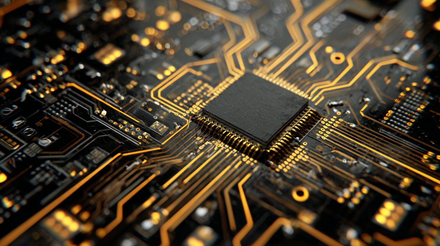
10 Secrets to Choosing the Best Printing Circuit Boards for Your Projects
In the ever-evolving landscape of electronics, the choice of Printing Circuit Boards (PCBs) plays a pivotal role in determining the success and efficiency of projects across various industries. According to a recent market report by Grand View Research, the global PCB market is expected to reach USD 83.1 billion by 2027, driven by advancements in technology and increasing demand for consumer electronics. As China maintains its position as a leading manufacturer, renowned for its innovation and quality, engineers and project managers must navigate a complex selection process to find the best PCBs that meet their specific needs. Understanding the critical factors involved in choosing the right PCB not only ensures high performance and reliability but also contributes to the overall success of electronic projects on a global scale.
Factors to Consider When Selecting PCB Materials for Future Technologies
When selecting PCB materials for future technologies, several key factors come into play that can significantly impact the performance and durability of electronic devices. First and foremost, the choice of substrate material is critical. Materials such as FR-4 and high-frequency laminates have distinct properties that cater to different applications, such as telecommunications or automotive systems. As the automotive PCB market is projected to grow at a rate of 5.9% from 2023 to 2032, understanding these material characteristics is essential for meeting the evolving demands in electric vehicles and advanced driver-assistance systems.
Additionally, thermal management is a vital consideration in PCB design. High-performance applications often generate excess heat, making it imperative to select materials with exceptional thermal conductivity. The integrity and reliability of a PCB can be compromised by inadequate heat dissipation, leading to failures in critical electronic functions. Furthermore, the rise of generative AI and other cutting-edge technologies necessitates robust PCBs that can support high-speed data transfer and layering capabilities. Thus, choosing the right PCB materials is not just about compatibility; it’s about paving the way for innovation in an increasingly competitive landscape.
Innovative Design Techniques for Improved PCB Performance in 2025
As we approach 2025, innovative design techniques are set to revolutionize the performance of printed circuit boards (PCBs). One of the most significant advancements is the integration of multi-layer designs that allow for increased functionality within a compact space. By stacking layers, designers can create more complex circuits without the need for additional board space, leading to enhanced performance and reduced weight—critical factors in industries such as aerospace and automotive.
Another exciting trend is the use of advanced materials that improve thermal management and signal integrity. Materials with higher thermal conductivity and lower dielectric loss are becoming the norm, enabling PCBs to operate at higher speeds and with greater efficiency. Techniques like embedded passive components are also gaining traction, allowing for a more streamlined design that minimizes interconnects, thereby reducing electromagnetic interference and enhancing overall reliability. These innovations not only optimize the performance of PCBs but also pave the way for more sustainable manufacturing practices as they contribute to reduced material consumption and waste.
The Role of Sustainability in PCB Selection and Alternatives
When selecting printed circuit boards (PCBs) for your projects, considering sustainability has become crucial in today's environmentally conscious landscape. Recent studies suggest that the electronics industry is responsible for nearly 70% of the world’s hazardous waste (Global E-Waste Monitor, 2020). As awareness surrounding this issue grows, manufacturers are increasingly focusing on sustainable practices, such as using eco-friendly materials and reducing harmful emissions during production.
One alternative that has gained traction is the adoption of bio-based or recycled materials for PCB manufacturing. For instance, the use of substrates made from recycled paper and bio-resins has been shown to significantly reduce the carbon footprint of PCBs, contributing to a circular economy. According to a report by the International Journal of Electronics and Communications, utilizing these sustainable materials can decrease energy consumption during production by approximately 30%. Choosing sustainable options not only aligns with regulatory standards but also appeals to a growing base of eco-conscious consumers. As the demand for green technology rises, opting for sustainable PCBs can set your projects apart while minimizing environmental impact.
10 Secrets to Choosing the Best Printing Circuit Boards
This bar chart illustrates the importance of various factors in selecting sustainable printed circuit boards (PCBs) for projects. Data reflects the percentage of importance attributed to each factor by PCB designers.
Analyzing the Impact of IoT on PCB Design and Manufacturing Trends
The integration of the Internet of Things (IoT) has significantly transformed the landscape of PCB design and manufacturing. As devices become increasingly interconnected, the demand for more complex, high-performance circuit boards has surged. Designers are now tasked with enhancing functionality while ensuring compactness, leading to the development of multi-layer PCBs that accommodate various components without compromising space efficiency. This evolution necessitates innovative design practices and materials to support the IoT's relentless march forward.
In response to this trend, manufacturers are adopting advanced technologies such as automated assembly processes and surface mount technology (SMT). These advancements not only streamline production but also elevate the quality and reliability of the final products. Additionally, PCB prototyping has become more crucial than ever, allowing designers to iterate rapidly and refine their prototypes based on real-world data. As IoT continues to shape consumer expectations and technological capabilities, staying abreast of these developments will be vital for anyone involved in PCB selection and manufacturing for their projects.
Emerging Technologies: How 5G and AI Influence PCB Choices
As technology evolves, the demand for efficient printing circuit boards (PCBs) is driven by advancements in 5G and artificial intelligence (AI). These emerging technologies are shaping the specifications and materials of PCBs, making it crucial for engineers and designers to understand their implications. For instance, 5G networks require PCBs that can handle higher frequencies and greater data throughput. This means selecting materials that offer lower dielectric losses and better thermal management, ensuring that devices can operate at optimal performance levels.
Moreover, AI integration into devices adds another layer of complexity to PCB selection. With AI’s reliance on data processing power, PCBs need to support high-density components and advanced circuit designs. This calls for not only innovative materials but also advanced manufacturing techniques like multi-layer configurations and embedded components. By aligning the design of PCBs with the principles of AI and 5G technology, engineers can create powerful, efficient, and future-proof devices ready to meet the demands of an increasingly connected world.
10 Secrets to Choosing the Best Printing Circuit Boards for Your Projects - Emerging Technologies: How 5G and AI Influence PCB Choices
| Aspect |
Description |
Importance |
Influence of 5G/AI |
| Material |
Type of substrate material affecting thermal performance |
High |
Enhanced materials for higher frequencies |
| Layer Count |
Number of layers in the PCB structure |
Medium |
More layers needed for complex circuits due to AI integration |
| Trace Width |
Width of the conductive paths |
Critical |
5G applications require precise trace widths |
| Component Placement |
Arrangement of components on the board |
High |
AI design tools optimize placement |
| Thermal Management |
Techniques to dissipate heat from components |
High |
5G increases power density, requiring better management |
| Signal Integrity |
Preserving the quality of electrical signals |
Critical |
AI helps predict and enhance signal paths |
| Cost |
Budget for production and material |
Medium |
AI can optimize design to reduce costs |
| Compliance Standards |
Regulatory standards the PCB must adhere to |
High |
5G certified standards may apply |
| Testing and Prototyping |
Process of testing designs for functionality and reliability |
High |
AI can automate testing to improve efficiency |
| Sustainability |
Environmentally friendly materials and processes |
Medium |
Emerging technologies encourage eco-friendly options |